You are here
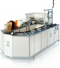
Manual and automated gauges for control of wafer thickness and geometry
Our capacitive based system can be used in many different applications. Generally, the systems measure distance, displacements and thickness of various materials.
Because of the use of a relatively low carrier frequency, in the case of silicon, there is no influence of the material's resistivity. The systems can be used in the entire range between 0,001 ohm-cm and 1.000 ohm-cm without calibration.
The semiconductor industry is now our biggest customer. Our different gauges can measure the Thickness, TTV, Bow, Warp and Stress.
Manufacturers of silicon wafers use E H gauges and sorters in every stage of the manufacturing process. In wafer fabs, among other applications, the systems are used to trace the variations in warp (stress) of processed and backside-ground wafers.
E H Metrology is also heavily involved in the growing Solar Industry.